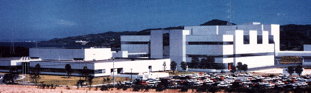
Fairchild decided in 1984 that we needed a plant in Japan, to more convincingly serve that market and to provide a window into Japanese manufacturing methods. I took over as Project Manager at the beginning of 1985. My right hand man was Dennis Walker, who is native Japanese, born in Nagasaki. Together we worked through two rounds of design with our architects Nikken Sekei. The first design was based on doing a minimal pilot line as part of the existing assembly facility in Isahaya, a town midway between the Nagasaki Airport and Nagasaki City. That project was truly sub-critical, so we did a design for a modern fab with 32,000 square feet of raised-floor clean room. The site plan supported a total of four buildings of that size. Of course, money started to run short, so only 1/3 of the total space was fully facilitized. However, the completed fab space was highly flexible, with two levels (6 meters total) available below the fab floor. Dirty equipment and outside access was segregated from the clean air return beneath the floor. The air flow was all down-flow, with flow rates determined locally by the HEPA density. For the equipment available at that time, this maximized the flexibility. Today, I would use Fan-Filter Units rather than big vertical vane-axial fans.
Ground-breaking was in late September, 1985, and the first good silicon was produced in early December, 1986.
By the time that silicon was produced, Fairchild was in doomed merger talks with Fujitsu. After the National acquisition of Fairchild was announced, Schlumberger sold the Nagasaki site with its front end and back end plants, to Sony. Sony took possession on January 1, 1988. They have subsequently developed the site to its full potential, and Nagasaki remains their flagship wafer facility.